
Quantum photonics in disordered nanostructures
After my PhD in the Material Science institute of Madrid, I obtained a postdoctoral position at the Technical University of Denmark and at the Niels Bohr Institute under the supervision of Prof. P. Lodahl, a worldwide expert on quantum photonics. In Denmark, I studied the role of fabrication imperfections in nanophotonic structures commonly used for quantum optics experiments: photonic-crystal waveguides and photonic crystals. Considering in particular on the study of light emission in these nanostructures at the single-photon level. These nanostructures are fabricated by etching nanometer-scale holes in a high refractive index semiconductor (GaAs) by using electron beam lithography and are widely used in the field of quantum photonics. A photonic crystal is a dielectric material that consists of a triangular periodic lattice of air holes etched in a high refractive index membrane (see Fig. c). The periodic lattice forms a frequency bandgap where light propagation is suppressed and light is confined in the third direction by total internal reflection. A photonic-crystal waveguide can then be created by omitting a row of air-holes in the periodic lattice (Fig. a). One of the most remarkable properties of these structures is that the material and fabrication process are compatible with the current growing techniques of self-assembled semiconductor light-emitting nanoscrystals. This allows embedding quantum light emitters in the form of semiconductor quantum dots or quantum wells directly in the semiconductor membrane. Scanning electron micrographs of these structures are shown in Figure a and c, respectively. My main goal was to understand the role of fabrication imperfections in these structures and to find alternatives routes to exploit disorder as a resource instead of as a nuisance.
Quantum photonics in disordered nanostructures 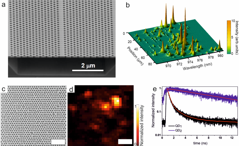
(a) Top view scanning electron micrograph of a photonic crystal waveguide made by etching holes in a GaAs membrane. By leaving out a row of holes it is possible to create a photonic crystal waveguide. There is (not shown) a layer of self-assembled InAs quantum dots in the middle of the membrane. (b) Even imperfections due to the fabrication process creates multiple scattering of light and an interference pattern of back and forward-propagating light that breaks the ideally guided mode into a set of random cavities along the waveguide. The emission from the InAs quantum dots fed all these random cavities along the waveguide when excited with an external light source. (c) Top view scanning electron micrograph of a disordered photonic crystal made by etching holes in a GaAs membrane. The scale bar is 1 micron. (b) Photoluminescence from InAs quantum dots embedded in the photonic crystal shown in (a), collected at a wavelength of (905 ± 1) nm under high-excitation power while scanning the structure. (c) Decay curves for two quantum dots at different positions in the photonic crystal with emission wavelength of 905 nm. The decay rate of QD1 (dark) is enhanced with respect to the decay rate of QD2 (blue) due to its spatial and spectral coupling to a disorder-induced localized mode. The decay of QD1 is 114 times faster than the decay of QD2. The same coupling can be obtained in the waveguide case. Images taken from references [Science, 327, 1352 (2010)] and [Phys. Rev. Lett. 109, 253902 (2012)].
Unavoidable imperfections due to the limited tolerance of the fabrication process lead to random multiple scattering of light with the lattice imperfections. This scattering process gives rise to strong interference effects which confines light in very small volumes, as shown in see Fig. b and d. This disorder-induced localization is dubbed after Philip Anderson who proposed the localization of the electronic wave function in a disordered solid as a mechanism driving the conductor – insulator phase transition random multiple scattering with the imperfections in the lattice [Phys. Rev. 109, 1492 (1958)]. These so-called Anderson-localized optical modes are very promising for cavity-quantum electrodynamics (QED) experiments where the radiative emission rate of single quantum emitters can be controlled when tuned through resonance with one of these random cavities, both in photonic crystal waveguides [Science, 327, 1352 (2010)] and photonic crystals [Phys. Rev. Lett. 109, 253902 (2012)]. These strongly localized optical cavities are revealed when embedding quantum emitters in the form of InAs quantum dots in these structures. By exciting these emitters under high excitation power, the photoluminescence emitted by the quantum dots feed the optical cavities which are then revealed while scanning the structures, as shown in Figs. b and d. When the emission frequency and spatial position of a single quantum dot matches those of a cavity, an efficient coupling is obtained which strongly modifies the decay dynamics of the emitter as shown in Fig. e. In this particular case, the position of the localized mode is depicted in Fig. d as compared to the photonic crystal shown in Fig. c. This particular structure contains InAs quantum dots at random positions with a density of 80 μm-2. Time-resolved spontaneous emission from quantum dots placed at different positions is performed by using time-correlated single-photon counting spectroscopy. Here, two different quantum dots are excited independently with a picosecond optical pulse and the emission time of single photons is recorded with an avalanche photodiode. After repeating the excitation-emission cycle many times (with a repetition rate of about 80 MHz), a decay curve of the emitted intensity versus time is obtained, from which the coupling to the photonic structure can be assessed and signatures of, e.g., Anderson localization are revealed. In this particular case, Fig. e plots the decay curve of two different quantum dots emitting at the same frequency as the Anderson-localized cavity but placed at different positions in the photonic crystal. While the QD1 is located very closed to the Anderson-localized cavity, QD2 is located further apart. The strong enhancement of the decay rate of QD1 with respect to QD2 (114 times faster) is due to the presence of the Anderson-localized mode.
Our experiments on photonic-crystal waveguides and photonic crystals demonstrated that unavoidable disorder due to the fabrication process is an efficient resource for confining light in nanophotonic structures, thereby opening a new avenue to all-solid-state cavity QED that exploits disorder as a resource rather than a nuisance. Exploring disorder to enhance light-matter interaction and establishing the ultimate boundaries for this new technology provide exciting research challenges for the future, of relevance to not only to QED but also other research fields that rely on enhanced light-matter interaction, such as energy harvesting or biosensing. Coupling several cavities is a potential way of scaling cavity QED for quantum information technology and represents one of the major challenges for engineered nanocavities. Controlled disorder might offer an interesting route to coherently couple cavities using so-called necklace states that are naturally occurring coupled Anderson-localized modes.